
blog

Technology Upgrade! Ruibo Automation Introduces Laser Flatness Measuring Instrument, Optical Ruler Empowers High-Precision Development of Domestic Semiconductor Packaging Equipment

Advanced Laser Metrology Accelerates Localization of Semiconductor Equipment With the rapid iteration and upgrading of the domestic semiconductor industry, the downstream market has set higher standards for the precision, stability and mass production capacity of packaging equipment, and high

Advanced Laser Metrology Accelerates Localization of Semiconductor Equipment

With the rapid iteration and upgrading of the domestic semiconductor industry, the downstream market has set higher standards for the precision, stability and mass production capacity of packaging equipment, and high precision, digitization and localization have become the core development trends of the semiconductor packaging equipment industry. To further consolidate the precision manufacturing capability of equipment, optimize equipment assembly processes, and enhance the core competitiveness of products, Shenzhen Ruibo Automation Equipment Co. , Ltd. (hereinafter referred to as “Ruibo Automation”) has completed the upgrade of core testing equipment, officially introduced a laser flatness measuring instrument, and fully applied it to the precision assembly and adjustment links of semiconductor packaging equipment, so as to help domestic semiconductor equipment advance to higher precision and higher efficiency with high-precision digital testing technology.

As a national high-tech enterprise and a “Specialized, Refined, Differential and Innovative” SME with years of deep cultivation in the semiconductor packaging sector, Ruibo Automation focuses on the R&D, production and sales of semiconductor packaging equipment, and has long been dedicated to the core technical fields of flip-chip packaging and ultrasonic welding, boasting a mature equipment R&D system and large-scale production capacity. The company features a rich and complete product portfolio, with various self-developed and manufactured precision packaging equipment that can be widely adapted to mainstream packaging processes such as TO, COB and COC, while fully covering the precision welding operations of various power semiconductor products. Leveraging stable equipment performance and mature technical accumulation, the company provides one-stop and full-process semiconductor packaging supporting solutions for industry customers, and has gained wide recognition from the market and clients after years of in-depth development in the sector.
For a long time, Ruibo Automation has always taken technological innovation as the core driving force for enterprise development, closely followed the development trend of the global semiconductor industry, accurately captured the refined production demands of industry customers, continuously increased R&D investment, and kept iterating and optimizing product structure, upgrading core processes and improving equipment performance. Relying on a professional R&D team and a mature technical system, the company has continuously broken through the technical bottlenecks in the precision manufacturing of semiconductor packaging equipment, continuously optimized the operation stability, adaptability and intelligence level of equipment, and consistently provided cost-effective and high-precision domestic equipment for the semiconductor packaging industry to help the industry reduce costs and increase efficiency.

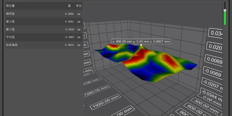
The laser flatness measuring instrument introduced this time is a high-precision testing equipment in the field of precision machinery manufacturing and equipment assembly and adjustment, which is specially built for high-precision equipment assembly and calibration scenarios. At present, this equipment has been fully put into the production and debugging process of Ruibo Automation, and is mainly used for the high-precision detection of straightness, parallelism and perpendicularity of the core structure of semiconductor packaging equipment as well as digital assembly and adjustment. Compared with traditional manual inspection and conventional instrument calibration methods, the laser flatness measuring instrument has multiple advantages such as high detection accuracy, data visualization, controllable error, and adaptation to precision parts inspection, which thoroughly solves the industry pain points such as precision deviation, vague data and poor repeatability in traditional assembly and adjustment processes.
Through the brand-new digital precision inspection and assembly & adjustment processes, Ruibo Automation has realized digitalized management and control over the entire equipment assembly process, which has significantly improved the overall assembly accuracy of semiconductor packaging equipment, effectively optimized the equipment assembly workflow, remarkably boosted assembly and adjustment efficiency, further reduced equipment operation errors, and guaranteed the precision, stability and durability of every finished equipment from the production source. This equipment upgrade is not only a comprehensive upgrade of Ruibo Automation’s production processes and quality control system, but also a key layout for the company to deeply cultivate the high-precision localized semiconductor equipment track.
Against the backdrop of accelerated localization of the semiconductor industry, precision manufacturing capability serves as the core for domestic equipment to break through. Going forward, Ruibo Automation will remain committed to the original aspiration of technological innovation, continue to introduce advanced precision testing and production equipment, constantly refine manufacturing processes, polish product quality, and optimize supporting services, keep making breakthroughs in core high-precision technologies for semiconductor packaging, continue to provide customers with higher-quality, more precise and smarter semiconductor packaging equipment and overall solutions, work hand in hand with industry partners for collaborative development, and pool efforts to drive the high-quality, high-precision and high-level development of the domestic semiconductor packaging equipment industry.

Related Recommendations

Comparison of G600 and G400 Precision Measuring Equipment: Same Micron-level Accuracy, Adapted to Differentiated Range Testing Scenarios

Select Optimal Laser Metrology Solution Based On Actual Measurement Demands In the field of guideway geometric accuracy calibration for precision machine tools, semiconductor and laser processing industries, the G600 and G400 series of measuring instruments, with their consistent core accuracy performance, cover the full range of long and short distance inspection scenarios. Both devices feature […]

Triple repurchase | We deliver the laser flatness measuring instrument again

Assist Dongfeng Equipment in upgrading its high-end intelligent manufacturing equipment Recently, the company successfully delivered and landed the third set of laser flatness measuring instruments to Dongfeng Equipment Manufacturing Co., Ltd. Three consecutive repeat purchase collaborations are not only highly recognized by customers for our product quality, measurement accuracy, and equipment stability, but also a […]

Empowering smart manufacturing upgrades with precision! Our laser flatness measuring instrument has been successfully delivered to Yunteng Laser

High-Precision Flatness Detection Optimizes Precision Laser Equipment Assembly Recently, our company has completed the delivery of a key equipment. The self-developed and manufactured laser flatness measuring instrument has been successfully delivered to Shenzhen Yunteng Laser Technology Co. , Ltd. , officially contributing to quality improvement and efficiency enhancement in the intelligent manufacturing of high-end laser […]